Table of Contents
Flash Profiling
This project is intended to explore the characteristics of the storage devices based in flash technology. The idea is to get a better understanding of the internals in this type of memory and create a model which allow a more effective use of these drives. To complete this task, we will create techniques that characterize the flash devices automatically. We will profile different devices, mostly SSDs, ranging from mobile- to enterprise-intended, SATA to PCI-e interfaces and sizes of 16GB to 70GB approximately.
Meetings
- 06/25/09: Sequential writes and modeling plan
- 06/22/09: Discussing new experiments with sequential writes w/ and w/o throttling
- 06/15/09: Alternative modeling options for write performance
- 06/09/09: Update on progress
- 04/29/09: One month plan and Sigmetrics paper discussion
- 04/07/09: Write Modeling and Initial Graphs
- 04/03/09: Modeling write latency
- 03/24/09: Write experiments discussion
- 03/20/09: Resolving write I/O issuing problem and some write modeling discussion
- 03/10/09: Modeling writes - some problems with profiling experiments
- 03/03/09: Modeling write latency and cleaning - graphs from Luis (not d2c)
- 02/17/09: Discussion about write profiling and SSD simulator
- 02/10/09: SSD Simulator experiments update
- 02/03/09: Logical simulator discussion
- 01/26/09: Using hardware simulator, logical vs. physical model, paper writing
- 01/09/09: Pre-UTC deadline discussion – plans for next submission
- 01/07/09: First full model discussion
- 01/05/09: Evening session: Explaning SanDisk Read graph
- 01/05/09: Afternoon session: paper discussion and task-list
- 01/02/09: Important discussion finally explaining the graphs and model refinement to incorporate this
- 12/31/08: UTC paper model discussion, layout, and applications
- 12/16/08: UTC paper motivation, layout, and experiments presentation
- 11/24/08: (Evening): Paper contents discussion and modeling read response times
- 11/24/08: (Afternoon): Analyzing read response time graphs
- 11/10/08: Discussion of read/write graphs and time-line experiments
- 10/27/08: Discussion on block size experiments and older pattern-size reads - in 2 parts
- 10/21/08: New flash-scheduler brainstorming and Block-size profiling discussion
Experiments
The following table shows the experiments that we will be performing in order to profile the flash devices. In each row is explained in very detail the parameters that should be used and varied. For all the experiments the Blktrace is taken and the phases time-stamp stored.
| Done? | Experiment name | OS Parameters | Exp. Parameters | Description |
|---|---|---|---|---|
| Yes | (1)Randop | Sched: Anticipatory, Async I/O | Write. Req. Size: from 1K to 1M. Delay: 0ms - 5ms - Sync | This experiments measure the impact that the delay have in merge and thus in the write performance of the SSD devices. |
| Yes | (2)Seg Simulator | Sched: Anticipatory, Async I/O | Write. Segment Size | Search for a better way of writing to the flash media. This experiment simulates the scenario where one segment in the flash is used as log for writes. After filled, a new segment is selected and the process repeated. |
| Part | (3)Part Simulator | Sched: Anticipatory, Async I/O | Write. # Parts 1-4 | This mimics experiment (2) but create several partitions each with one log. This experiments explores if having this writing method improve the write performance in flash devices. The rational behind this experiment is the parallelism inherent to flash technology. |
| No | (4)# Parallel Units | N/A | Async I/O Read. Access-gap between requests | Characterize the matrix of parallel units that composed the profiled flash. The output of this experiment will be the response time for each pair of request sent. It is clear that, if the requests have to be serialized, then they will have a higher response time that the rest of the cases. |
| No | (5)SSD queuing system | Same as (1) | Extract the queuing capabilities of the SSD: Merging, sorting, etc. To execute this experiments we should be able to eliminate the OS I/O Scheduler by eliminating the Plug/Unplug system or shrink the device request queue to 1. We could perform the same set of experiments as (1). | |
| No | (6)Host Overhead | N/A | Finds the overhead time in the transfer from the media to the host. Assuming that the device include a read cache, we could perform two synchronous requests and measure the difference between response times for both requests. | |
| No | (7)Page Size | N/A | Request Size | We know that the write unit in the Flash devices is at the page granularity. This means that, in order to write part of a page, it is required to perform a read/merge/erase/write operations sequence. We could perform an experiment where we start writing to the LBA 0 and then increase the request size and repeat the experiment. For some request size, the response time of the write will be smaller than the others. This size will be a clear indication of the page size. |
| No | (8)Block Size | N/A | After knowing the page size, we write to the device with requests of size equal to the flash-page sequentially. One of this requests will take longer since the SSD has to perform an erasure operation. Then, we will know that the first page of another block has been reached. Thus, we can conclude how many pages compose a Block consequently we know the size of one block. | |
The following table lists details of the graphs that we should do as part of the profiling from the results obtained in the experiments above. The intention of each of this graphs is to uncover non trivial characteristics of the Flash profiled.
| Done? | Description |
|---|---|
| Part | Plot size of the request vs. throughput for all the different delay models from the results of experiment (1). This graph will show the impact of having an small delay between requests. In order to have a complete picture of the results, we also need to show the ratio of merging given by btt. |
| Yes | Plot size of the segment vs. the throughput for the results in experiment (2). This could be done for different delay times between requests. |
| No | Plot number of partitions vs. throughput for results in experiments (3). As in the previous cases, a delay could be added and plot the different lines. |
| No | Plot access-gap vs. response time. This graph should give a good idea of the positions in the flash of the parallel units. |
Randop
First, we construct a micro-benchmark called randop. This tool issue asynchronous I/O requests to the device being tested. It varies two values in the requests creation: request size and access-gap. The output of the experiments is the throughput in MB/sec averaged from 5 experiments. The throughput is carefully measured by accounting just the time when at least one operation is outstanding. The standard deviation is also computed and plotted. randop ensures that, in all the variations, the devices receive the same amount of data to avoid false results when, for instance, the cache services all the requests avoiding the actual disk operations.
Sequential Write
We use randop to execute this experiment. The next graph shows the impact of having different delay times. The standard deviation is not plot since is very small with an average of 0.74. It is clear that, even when you have a small delay as 1ms, the performance and opportunity of merging in the I/O scheduler is greatly decrease. However, this results improve when the total requests size reach 256 KB in size.
With BTStats
Segment Simulator
One idea in order to improve the write performance of the flash is to select a segment and write in it all the incoming requests sequentially. In order to test this approach, we implemented a simulator. seg_simulator perform asynchronous operations over the flash by selecting a random segment and write it sequentially. Then, a new segment is chose and the operations repeated. This micro-benchmark varies the segment size and also evaluate the impact of different delay time between requests. The following figure shows the throughput of two experiments: one with no delay and one with random delays ranging from 0 to 5ms. The requests size was set to 4 KB, the most common request size in the Linux kernel.
Partition Simulator
Based on the flash internal composition, we could derive the possibility to send multiple requests to different segments or parts to parallelize and get better performance. For that reason, we construct a simulator which writes to the SSD varying the number of partitions where it will send the requests. For each partition we will have a segment as described in the last subsection. Then, the selection of the next partition segment to write will be done in a round robin fashion. The following graph shows the results for this experiment:
Pattern Size
After trying to use the algorithms presented in the paper of Desconstructing RAID systems in order to find the patter size of the flash devices, we realize that all the SSDs in our use did not support Command Queueing that is an assumption in this experiment.
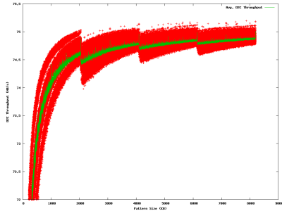
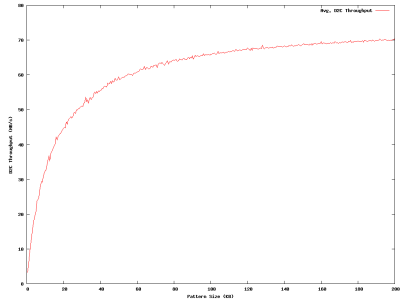
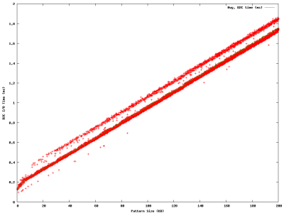
We developed a new algorithm in order to find this parameter of the SSDs. It consists of sending requests of size of the assumed pattern size and let the internals of the SSD split them to be served by multiple parallel units. We increase the assumed pattern size up to 8MB. For each pattern size we repeat the experiment 50 times.
Samsung SSD
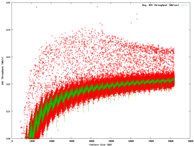
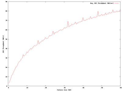
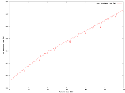
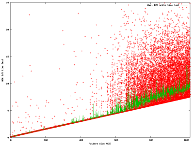
Below I show the graphs obtained for the samsung devices. The throughput and response time of each experiment is presented.
Derivatives
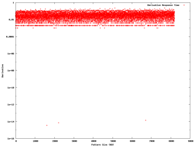
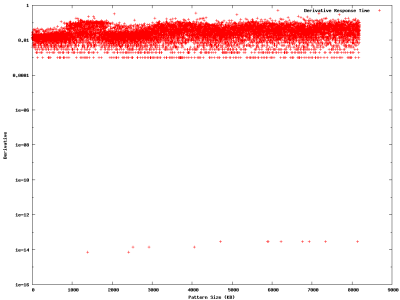
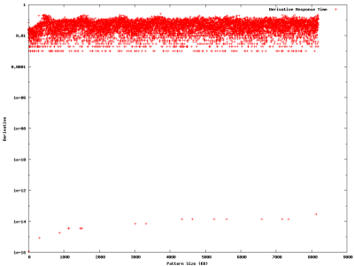
Although these graphs show that there is a clear pattern size of 256KB, If we plot the same graph with a much more small scale, we can see that there are also more hidden pattern size at this scale.
Write
Sandisk SSD
Derivatives
Write
MemoRight
Derivatives
Write
Parameters
This section contains a list of parameters that are deemed to be most relevant to collect from SSDs within the scope of this project. We guided our selection of parameters according to their impact in two main areas: i) performance (P), ii) reliability (R). This is an open list, though; we shall consider other areas as the project goes on. The parameters are further classified in categories.
| Parameter | Related Experiment | Area | Description |
|---|---|---|---|
| Size | |||
| (1) page size | (7)Page Size | P,R | SSD unit of read/write operations. |
| (2) block size | (8)Block Size | P,R | SSD unit of erase operations. |
| (3) #of par_units | (4)# Parallel Units | P | SSD degree of parallelism, that is, the maximum number of page reads that can be executed without incurring in serialization penalties. |
| (4) #of planes | Not available | P,R | Samsung's SSD specific - a plane is a set of blocks |
| (5) #of dies | Not available | P,R | Samsung's SSD specific - a die is a set of planes |
| (6) #of flash_pkgs | Not available | P,R | Samsung's SSD specific - “A flash package is composed from one or more dies (also called chips).” |
| (7) map granularity | Not available | P | Mapping granularity: {page, block, …} |
| Cost | |||
| (8) page/block read cost | (6)Host Overhead | P | Time it takes to read a page, respectively a block, from SSD into the OS user space. |
| (9) page/block write cost | Not available | P | Time it takes to write a page, respectively a block, from OS user space to SSD. |
| (10) block erase cost | Not available | P | Time it takes to erase an SSD block. |
| (11) page access cost | (6)Host Overhead | P | Time it takes to read a page from SSD into SSD read buffer. Note we can derive host overhead by substracting page parameters (8)-(11). |
| Throughput | |||
| (12) random read/write throughput | (1)Randop | P | Throughput for random read/write patterns of various request sizes. This is a table. |
| (13) sequential read/write throughput | (1)Randop | P | Throughput for sequential read/write patterns of various request sizes. This is a table. |
Tentative parameters for which no specific semantics has been defined yet:
- Free space cost
- Wear leveling efficiency
Abstract SSD Model
This section presents an SSD abstraction under certain assumptions. A hierarchical architecture is proposed, and the concept of parallel units is formalized.
Assumptions
1.1. An SSD exposes a logical block interface to the OS, and it is composed of an array of Flash Packages (FPs.)
1.2. There is Flash Translation Layer (FTL) component that maps logical blocks to physical locations in the SSD. The mapping may change as data is written into the SSD or internal maintenance mechanisms occur (e.g. relocation of data to reclaim free space.)
1.3. The SSD has a controller, with minimal CPU and memory, to run firmware to run firmware (implementing FTL logic, and other modules.) [3: pp. 4] [5]. The SSD controller is in charged of managing the FP array.
Is this really important? Why?
*1.4. A page is the minimum amount of data that can be read or written from or to the medium respectively [4: pp. 35(read), 36(write)].
1.5. A physical block is a list of B physically contiguous pages, numbered 0 to B-1 [2] [4: pp. 8].
1.6. No allocated page can be overwritten in place before first erase the block container [4: pp. 36].
1.7. Data is erased at physical block-sized units, called the erase unit [4: pp. 38].
*1.8. A logical block is a list of L pages logically numbered from 0 to L-1. These pages may or may not be allocated contiguously in the medium. [2]
* Are to be confirmed as more supporting documentation is found.
References
[3] MTRON SSD MSD-SATA3035 Product specification.
http://www.mtron.net/upload_Data/Spec/ASiC/MSD-SATA3035.pdf
[4] Samsung FLASH MEMORY K9F8G08UXM specifications.
[5] Sandisk SSD 5000
http://www.sandisk.com/Assets/File/pdf/industrial/SanDisk_SSD_SATA_5000_2.5_DS_Rev0.2.pdf
Flash Memory Hierarchical Architecture
There is a hierarchy of physical units: PU1, PU2, …, PUh
PU: Parallel units?
We do mean “Physical Units.” We should think of them as tangible objects in the SSD, e.g. a physical page.
Where:
- PU1 is the smallest allocation unit
- PUh is the whole SSD
- PUi is composed of many PUi-1, j with i=2, 3, …, h and j=1, 2, …, Ni
This bullet is not clear.
You build a PU by using smaller PUs as building bricks.
- A given PUi-1 belongs to only one physical unit PUi.
Does this mean that there is no remapping of lower PU's into higher PU's?
Physical Units are not remapped or moved since they are soldered in the FPs. Logical units are certainly remapped.
Examples include:
- PU1 = Page
- PU2 = Block
Other examples:
- PU3 = Plane; PU4 = Die; PU5 = Flash Package; PU6 = SSD
Parallel Units
A. Parallel Compatibility

Two different physical units u1 and u2 with the same hierarchical level i may be (read/write) accessible simultaneously, e.g. there is no shared interconnect to the SSD controller or serialization mechanism that prevents simultaneous updates to both units. We then say that “u1 is parallel compatible with u2”, or equivalently: (u1║ u2).
Then, the total read/write throughput is calculated as the addition of individual physical unit throughput.
Total Throughput (u1║u2) = Throughput(u1) + Throughput (u2)
Can we generalize this as a sumation? <latex>\sum_i T(u_i) </latex>
Yes. I will put a math statement shortly.
B. SSD parallel Units
The cardinality of the minimal subset of parallel compatible units {ui, j} with i=1, 2, .., h and j=1, 2, .., pi that has maximal throughput is the number of read parallel units in the SSD and its corresponding SSD read throughput. Likewise for writes.
Notes
- In “A”, write operations may be effected by other factors, e.g. allocation pool, mapping granularity, which we’ll refine in next iteration.
- In “B”, minimal/maximal wording needs to be simplified for the sake of compactness and clarity.
Allocation Pool
For all u1, u2: ( u1║ u2)
For all random updates w1 є {random writes on u1} U {no update},
For all random updates w2 є {random writes on u2} U {no update}
If u1'= w1( u1)║ u2'= w2( u2)
then free-block allocation pool AP1 is of size less than or equal to u1, respectively AP2 in relation to u2.
Mapping Model
There are many ways in which the FTL can map blocks from the logical address space into the SSD physical storage units. At the same time, SSD wear leveling strategies influence how free blocks are allocated along the entire storage space – allocation pool management, as well as how used blocks are moved around during random updates.
We will initially concentrate on the mapping scheme. Later on, we will attempt to measure the effects of wear leveling mechanisms in the assumed mapping model. We can identify the following mapping schemes:
Striping scheme
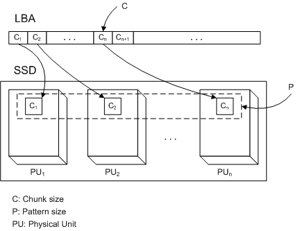
It is similar to RAID-0 arrays in which each storage unit is assigned equally-sized contiguous LBAs, called a chunk, in a round-robin fashion, forming a full stripe altogether. The chunk size could be anything from a single 512-Byte logical block to larger ranges of LBAs.
Pictorially:
Range scheme
The LBA space is partitioned in two or more ranges or segments, and each range is mapped to physically contiguous SSD storage space. E.g. a 1GB flash memory made up of two planes can have the LBA divided in two 512MB ranges, each one of them assigned to a plane.
Pictorially:
*Hashing scheme
A hash function is applied to the LBA to determine its physical SSD storage location. The FTL should manage collisions, and bad-sector assignments.
Algorithm
In the following algorithms, we assume the mapping model follows the striping scheme.
Pattern Size
Same as RAID paper. Some algorithm variations may be necessary to accentuate the serialization latency, e.g. reading extra pages in the offset vicinity, if no clear pattern emerges.
Chunk Size
Same as RAID paper. Alternatively, Experiment #2 Seg Simulator may provide initial estimation.
Page Size
Assumptions
- A1 - Every C-sized chunk is allocated on physically contiguous SSD pages.
- A2 - Partial page reads take about the same time as full page reads.
- A3 - Reading two physically contiguous pages takes twice as much as reading one of them.
Algorithm
Input - SSD LBA space, chunk size C
Output - SSD page size
1.  Divide LBA space in C-sized segments
2.  p=512 // p is the assumed page size
3.  RT_prev=0, RT_curr=0 // response time variables.
4.  While (p < C AND NOT(RT_curr ~ 2 * RT_prev))
5.    For j in 1..R
6.      Choose N random segments {Si} i=1,…,n
7.      Parallel read p-sized data starting from first byte
        in every Si, and measure response time in RT[j]
8.    end for
9.    RT_prev = RT_curr
10.   RT_curr = Average(RT[] array)
11.   if (RT_prev == 0)
12.     then RT_prev = RT_curr // first iteration
13.   p = p + 512
14. end while
15. if (p < C)
16.   then Page Size is (p - 512)
17. else
18.   Page Size is C
The algorithm issues N asynchronous random reads of size p – the assumed page size, starting from 512 Bytes in Line 2, and measures completion time. It repeats this step R times in Lines 5-8, and averages completion times in Line 10. Then gradually increases the assumed page size by 512 Bytes in each iteration.
If p is less than the actual pages size, response times of p-sized IO reads, i.e. partial page reads, will be comparable to smaller IO requests per assumption A2.
The rationale is that as soon as p spans more than a single page, the response time in Line 10 will be doubled as compared to the previous iteration per assumption A3. Then, we say the page size is the value of p in the previous iteration.
If previous and current average response times keep being comparable, and p exceeds C, then page size is said to be equal to C.
Open issues
- We need to claim if some specific scheduler is required.
- Required: Devices information table
- Required: Devices profile table
- We have to state our flash model.
- How can we use the results from the profiling?
SVN Repository
The checkout command for the repository of this project is:
svn co https://doomsday.cs.fiu.edu/svn/flash_profile
The structure of the folder is as follow:
- experiments: Include all the relevant experiments I have done for the flash profiling work. Each inner directory correspond to one experiment. All of them have a graph directory that contains their results. In the graph directory there exist one directory per device. The experiments are:
- blk_size: Experiment to find the block size of the device. This creates a response time time-line for various request size.
- dev_overhead: Find the overhead of issuing a command to the device taking advantage of the read-cache.
- seg_pat_size: This implements the experiment explained in this section.
- papers: Papers for this work.
- presentation: Presentation for Jason Liu when joined the team.
- fast09: Paper sckeleton for FAST09.
seg_pat_size
Inside each device directory for the seg_pat_size experiment, you will find some files ending in _complete. This files correspond to the complete data-points that you see in the graph. Each column represent:
(ignore this) (response time (ms)) (throughput (MB/sec)) (pattern size (KB))
All this information is obtained with the D2C events.

